KICAD TUTORIAL Make Your First Printed Circuit Board


Why Learn PCB Design?
When I started building circuits as a teenager, I used different types of prototyping boards. I only built circuits with few components because of all the wires I had to solder here and there to get it working.
I remember finding cool projects with circuit diagrams included. Like guitar effect pedals. Or DIY weather stations. And I really wanted to build them.
But all of them needed at least 20-30 components. Usually much more. So I didn’t dare to try as I knew that I would end up with a big mess of wires, almost impossible to troubleshoot. And even if I’d be able to do it, I’d be afraid to use it in real life in case I would mess something up.
It wasn’t until my early twenties that I first tried to design my own custom Printed Circuit Board (PCB). And after that, I was hooked! The number of components for a project wasn’t a problem anymore. I felt I could build anything!
When you design your own custom PCB, you’ll draw the connections in peace and quiet on your computer. You can double and triple check your connections easily. You even get help from the design program to check for errors.
Next, you can get a few copies of your board made for just a few bucks.
Now you have a board in hand that you know have all the correct connections. No wires needed. All you need to do is to solder the components to the board, just like a soldering kit, and your circuit should work.
In this kicad tutorial, you’ll learn how to make your first PCB. I’ll show you by creating a super simple project in KiCad. After you’ve done one project, you’ll know the basics and can design more PCBs on your own.
But if you want more instructions, more projects to try, and a place to ask questions and discuss electronics projects – I also invite you to check out my electronics community Ohmify:
So, let’s jump right into it!
1. The Software: KiCad
There are several software alternatives for designing PCBs. KiCad is a free and really good alternative. It’s used extensively by both hobbyists and professionals. That’s what we’ll use in this tutorial.
KiCad is available for Windows, macOS, Ubuntu, and many other platforms. Find the platform alternatives and download the installation files for KiCad here:
- Download and install KiCad
2. Starting a New Project
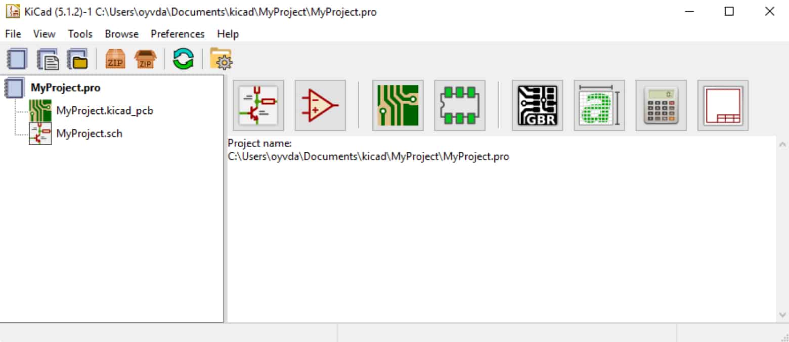
When you open up KiCad, you’ll see the window shown in Image 2.1. From here, you can open or create new projects.
To create a new project, click on the File menu and select New -> Project.
Choose where you want to save your project and type in a name for it. Then click on the Save button.
Your new project will be empty. It’s now your job to first create a schematic, then later draw the board layout.
You create the schematic from the Schematic Layout Editor, also called Eeschema.
Open the editor by double-clicking on the schematic file on the left, or by clicking on the Schematic Layout Editor button (Image 2.2).

Schematic layout editor button
When opening the editor for the first time, you might get asked to Configure the Global Symbol Library Table.
Just choose the recommended settings.
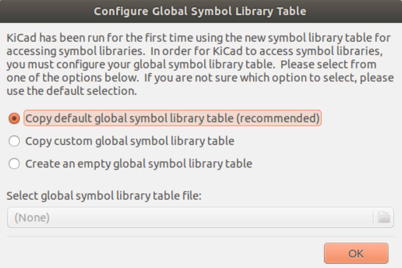
NOTE: If the recommended option is disabled, it most likely means
that you installed KiCad without the default libraries. In that case, you need to download and install the libraries manually. Learn more about that here:
https://forum.kicad.info/t/library-management-in- kicad-version-5/14636
- Create a new project
- Open the Schematic Layout Editor
3. Adding Components
Your schematic is where you draw your circuit. First, you add the components you want. Then you add wires to show how to connect your components.
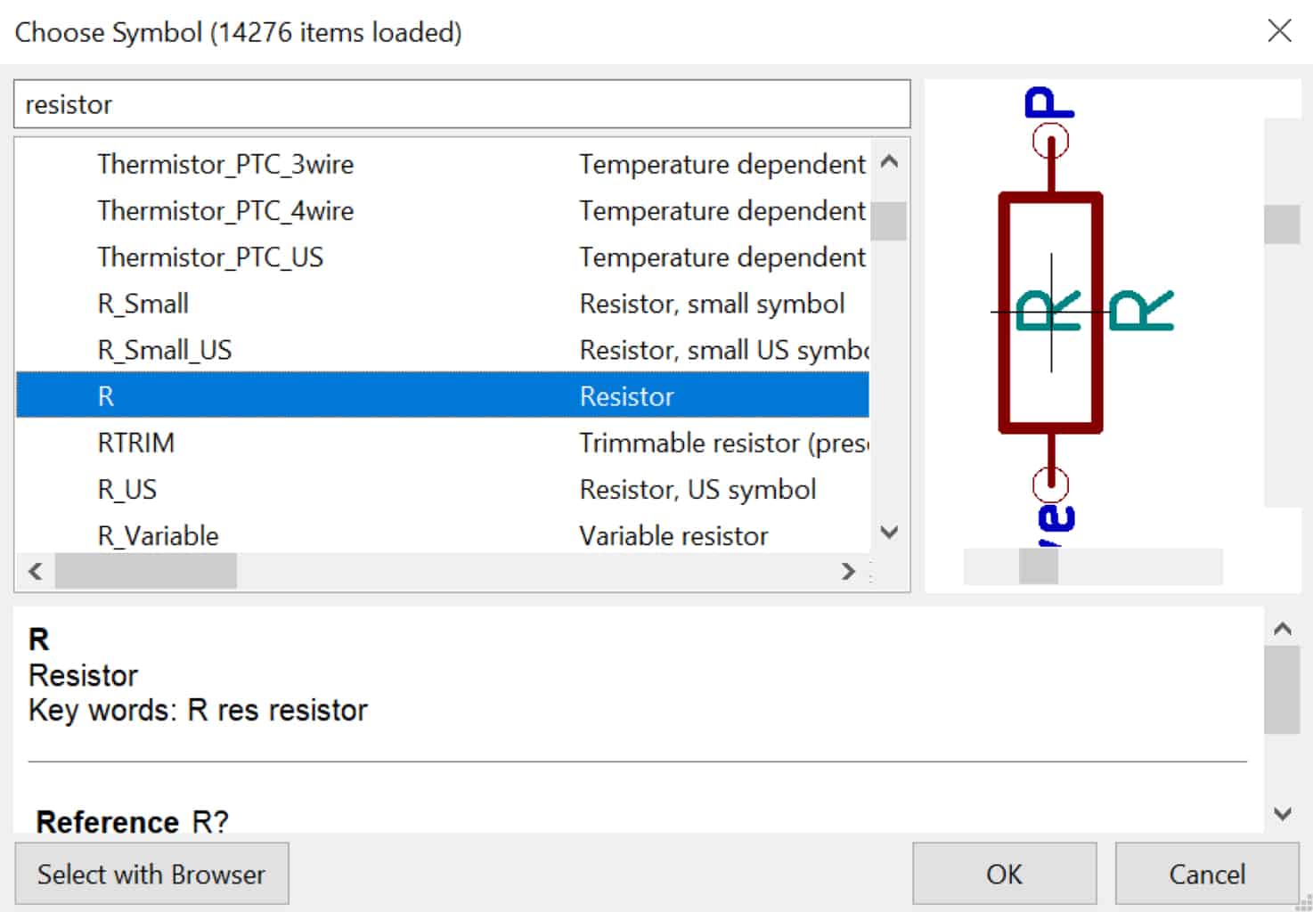
To add a component, click on the Place Symbol button on the toolbar on the right (or press A on your keyboard), then click anywhere in your work area. This brings up the component chooser.

The place symbol button
From the component chooser, you can search for the component you want to add. Just type in what you’re looking for. For example, if you need a resistor, type in “resistor.” Look through the list of results and choose a good match *.
* What is a good match?
The most important thing is that you choose a symbol that represents the component you want to use in the best way possible.
For example, when you search for “resistor,” you’ll get several options like “thermistor,” “trimmable resistor,” and such. But you also get a symbol that is just a resistor, nothing more. So that’s the best representation.
Place the symbol
When you’ve chosen a component, place it in your schematic by clicking in your work area with your mouse.
If you later want to move the component, place your mouse pointer over it and press M on your keyboard. To rotate the component, press R. You can zoom in and out by using your mouse wheel – or F1 and F2 on your keyboard.
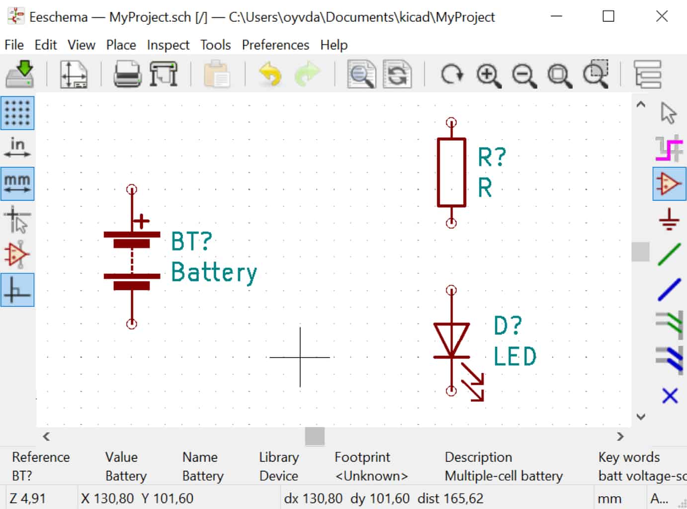
- Add a resistor, an LED, and a battery to your schematic
- Move the components so that they are positioned the same way as in Image 3.3
4. Adding Wires
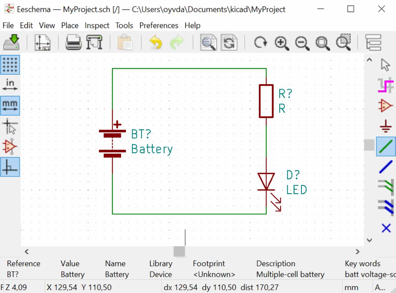
Now you need to draw wires between the components to connect them. You can do this by clicking on the Place Wire button on the toolbar – or by pressing W on your keyboard.
The Add Wire Button
Click on the pin of a component to start drawing a wire. Then click again on the pin where you want the wire to end.
If you want to move a component now that they are connected, you have two options: Move and Drag
If you place your mouse pointer over a component and press M on your keyboard, you Move the component without the wires. But if you press G, you Drag the component with the wires attached.
If you start moving or dragging a component but then change your mind, just press the Escape key on your keyboard to release.
- Draw wires between the components so that you connect them like in Image 4.2
- Test out the two methods of moving a component (Move and Drag) after you’ve connected them
5. Adding Symbol Values
In most cases, a component should have a value. For example, a resistor should have a resistance value. A battery should have a voltage value, etc.
By pressing V on your keyboard, with your mouse pointer over the component, you can edit its value. You also find this option in the menu when right-clicking on the component.
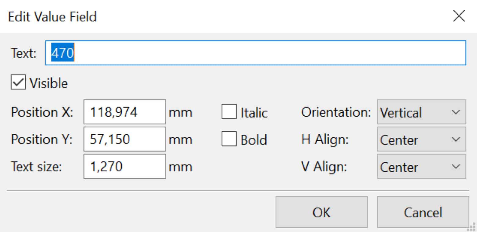
To set a resistor value to 470 Ω, you’d normally write “470”. And to set the battery value to 9 volts, it’s normal to write “9V”. For the LED you could, for example, write “2V RED” or something similar to indicate that you want to use a red LED with 2V forward voltage.
Note that the value you set for a component does nothing to your circuit. It just serves as a reminder for you, so that you’ll remember what value to use when you build the circuit.
- Add "470" as the value for the resistor
- Add "9V" as the value for the battery
- Add "2V RED" as the value for the LED
6. Annotating the Schematic
The next step is to Annotate your schematic, which means to give the components a unique identifier. For example, if you have several resistors, they will be named R1, R2, R3, and so on.
To do this, click on the Tools menu, then choose Annotate Schematic.
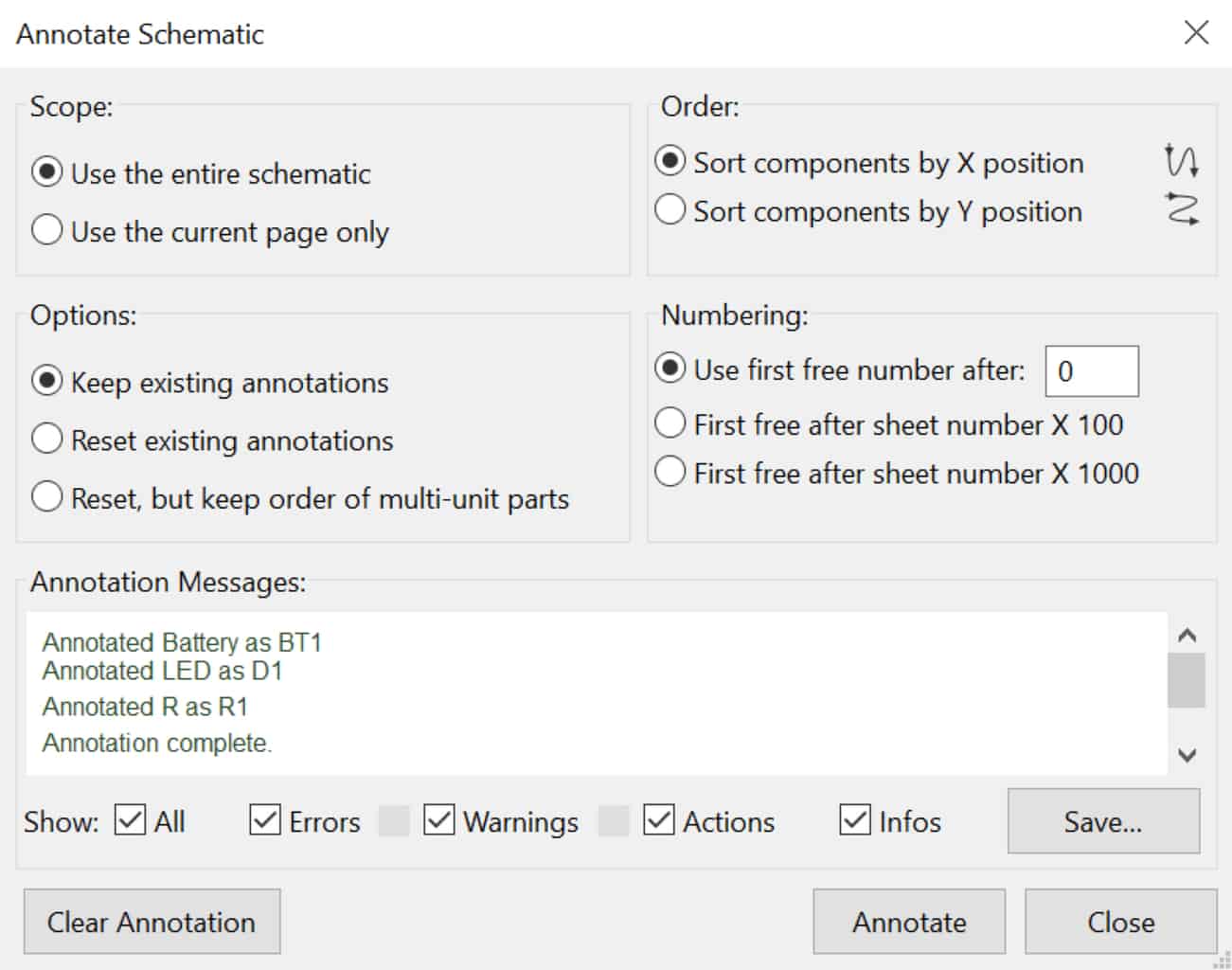
Leave the default options and click on the Annotate button. Then close the window.
Now you can see that the components have numbers: BT1, R1, and D1.
- Annotate your schematic
7. Adding Footprints
Before you can move on to drawing your board, there is one more thing you need to do; add footprints to your components.
The footprint is what will be printed onto the board for each component.
For example, for a through-hole resistor, you’ll choose a footprint with two holes, so that you’ll get two holes for soldering the resistor onto on your board.
Click on the Tools menu and choose Assign footprints…
Sometimes it takes a bit of time to load all the libraries, so be patient.
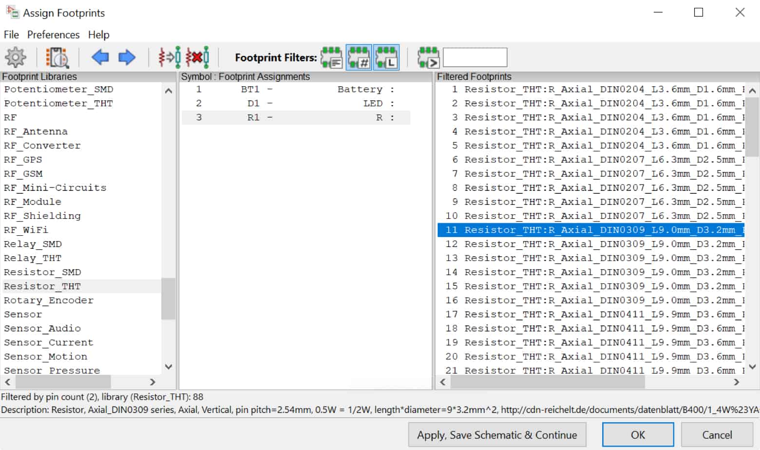
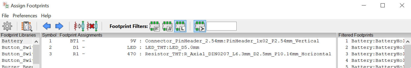
Image 7.1 shows the footprint selector. On the left side, you see all the footprint libraries you have available. In the middle, you have the components from your schematic. And on the right, you have a list of footprint options to choose from.
To see what a footprint looks like, right-click on it and select View Footprint.
Filters help you narrow it down
There are a lot of footprints in KiCad.
But on the toolbar, you have filters to choose from to help you narrow down your options:

The Footprint Filter Selector
If you filter by pin count you’ll only see footprints that have the same number of pins as your component.
If you filter by library you’ll only see footprints from the library that you have selected on the left.
The schematic symbol footprint filter will filter based on filtering rules set by the symbol.
What footprint to choose for the battery?
There are many ways to connect a battery. You can use a battery holder that’s fixed onto the board. You can use a barrel connector. Or how about two pins?
For 9V batteries though, I prefer using a battery clip. It’s a clip you fasten to the top of the battery that has two wires going from it.
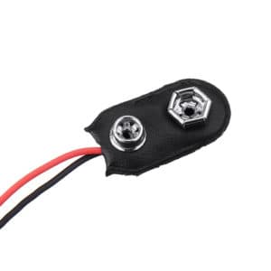
Such a clip doesn’t exist in KiCad at the time of writing. But all you need is a couple of holes where you can solder the wires from the clip. If you add a pin header with two pins, the footprint will be two holes.
You can find pin headers for example in the Connector_ PinHeader_2.54mm library.
There are a few options here. Have a look at a couple of them by right-clicking and choosing View Footprint. Then click on the 3D Display button to see what it looks like in 3D.
Remember that it doesn’t matter which one you choose, as long as it adds two holes to your board. Double-click a footprint to choose it.
What footprint to choose for the resistor?
You’ll find two resistor libraries among the standard KiCad libraries: Resistor_THT and Resistor_SMD.
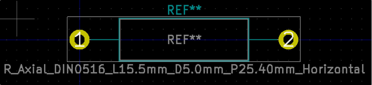
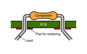
THT stands for Through-Hole Technology. That’s the type of component where you put the legs into holes on the board and solder on the other side as shown in Image 7.5. It’s the classic type of component, often used by hobbyists as it’s a bit simpler to solder.
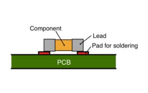
SMD stands for Surface Mount Device. That’s the type of component that lies on top of the board. You solder them on the same side, as shown in Image 7.6. SMD is the standard component type for modern electronics. They are smaller and take up less space.
For this circuit, let’s use Through-Hole Components, so select the Resistor_THT library.
There are tons of options. But note that it’s not very important which option you choose here. All of them will give you two holes on the board to solder your resistor into.
But if you want the perfect fit, measure the resistor you plan to use – or look at its size specification from the store where you plan to buy it. Then choose the closest match you can find.
What footprint to choose for the LED?
The last component is the LED. Choose the LED_THT library to add a through-hole LED.
A typical LED is 5mm in diameter. There are many 5mm options in the library. A lot of them have the same footprint but different 3D models. Have a look at the 3D version of a couple of them to get an idea of the difference. (Right-click and select View Footprint. Then click on the 3D Display button.)
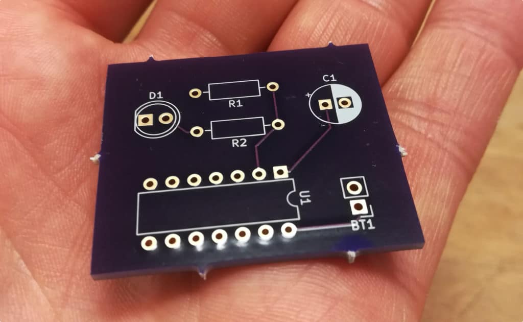
Double-click to choose one. You can see my footprint selections in Image 7.7.
- Add footprints for the resistor, the LED, and the battery. See image 7.7 for my selections
8. Running the Electrical Rules Check
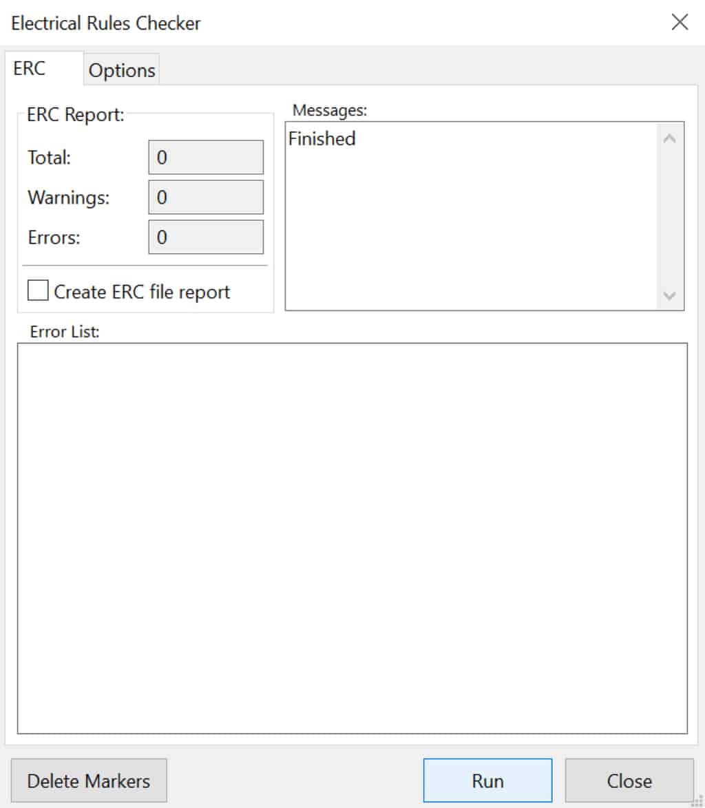
It’s easy to make errors, like forgetting to connect a component. Especially when you are drawing large circuits. To help you find these errors, use the tool Electrical Rules Check (ERC).
Click on the Inspect menu and choose Electrical Rules Check. Or click on the Perform Electrical Rules Check button shown in Image 8.1.

The Perform Electrical Rules check button
In the window that pops up, click on the Run button and look for error messages under Error List.
A typical error here is if you forgot to connect the pin of a component to another component. Or if you accidentally moved a component so that it’s no longer connected.
If there are no errors, you’ve finished the first phase of drawing the schematic. You can move on to the second phase – designing your board.
- Run the ERC and fix any errors that appear
9. Schematic Design Checklist
That’s it for drawing the schematic. To make it easier for your next design, here’s a checklist with all the action points you need to take before moving on to the board design:
- Add all components to your schematic
- Connect all components with wires
- Add values to all components
- Annotate your schematic
- Add footprints to all components
- Run the Electrical Rules Checker (ERC) and fix any errors
10. Starting a New Board Layout
You have defined how you want to connect the components in the schematic editor, and now it’s time to put that onto your board. You need to decide where to place the components, then draw tracks to create the connections between them.
To start drawing your board layout (assuming you’re still in the Schematics Editor), click on the toolbar button that says Run Pcbnew to layout printed circuit board, as shown in Image 10.1. Or go to the Tools menu and select Open PCB Editor. This opens up the Board Editor window.

The button to go from schematic design to board layout
The first thing you’ll see is just an empty area.
To get started, you need to retrieve information about footprints and connections from your schematic. You can do this by clicking on the toolbar button that says Update PCB from schematic… as shown in Image 10.2. You’ll also find this option in the Tools menu.

The button to update PCB from schematic
A window will pop up.
Keep the default options and click on the Update PCB button. This will load your footprints. Then click on the Close button.
Click anywhere to place the components.
If you zoom in on the components, using either your mouse-wheel or F1/F2, you’ll see white straight lines between the pins. These are called air-wires and tell you which pins to connect – according to your schematic.
- Update your PCB from schematic, so that you see the three footprints you’ve chosen
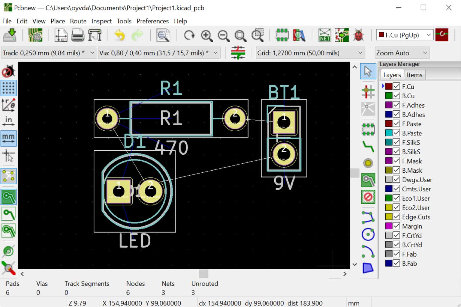
11. Positioning the Components
Your next task is to position your components so that it becomes easy to connect the components according to your air-wires. If you’re able to place the components in a way that no air-wires cross, that’s the easiest.
I recommend positioning the components like the way you did in the schematic, if possible. It’s not very important for such a simple board, but for more complicated boards it can simplify troubleshooting.
To move a component, move your mouse over it and press M. If you already have a group selected, the whole group will move. To deselect the group, press ESCAPE. To rotate a component, press R.
If you accidentally place your mouse over the component name, you’ll move only the name. Just press ESCAPE to try again.
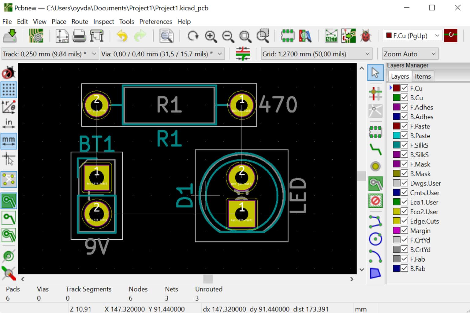
- Place the components in an orderly way, similar to the way you placed them in your schematic diagram
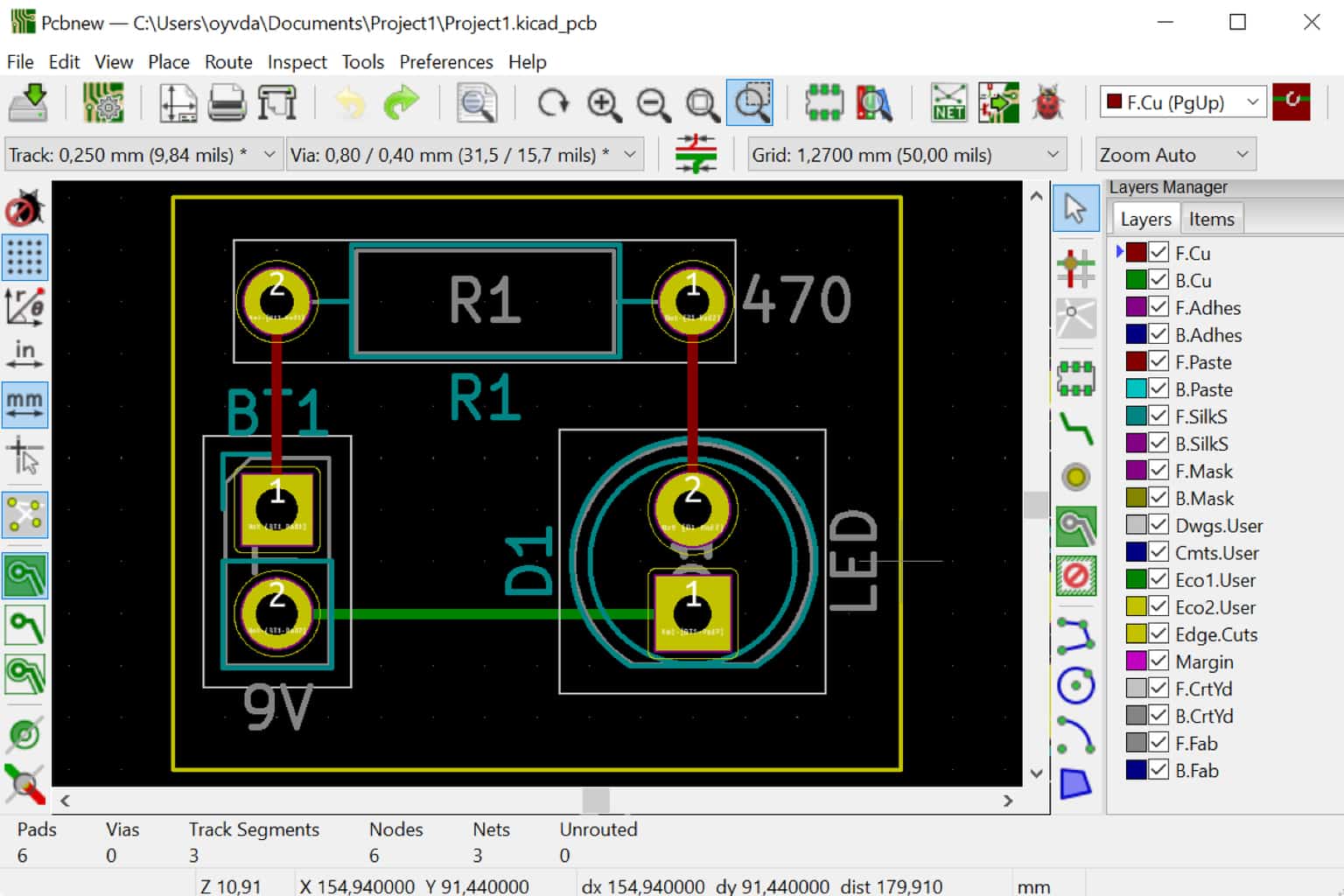
12. Drawing the Tracks
When you’re happy with the placement, the next step is to replace the air-wires by drawing tracks to connect the components. The tracks you draw will become copper traces on your finished board.
Start drawing tracks by clicking on the Route Tracks button on the toolbar on the right (shown in Image 12.1) – or press X on your keyboard.

The button for routing tracks
You can choose if you want to draw on the front or the back of the board, by selecting a layer in the Layer Manager. The little blue triangle on the left shows the selected layer.
- F.CU is the front (or top) side.
- B.CU is the back (or bottom) side.
Click at the beginning of an air-wire to start drawing a track. Click again where the air-wire ends to finish drawing the track.
When there are no more white lines, you’re done routing the tracks.
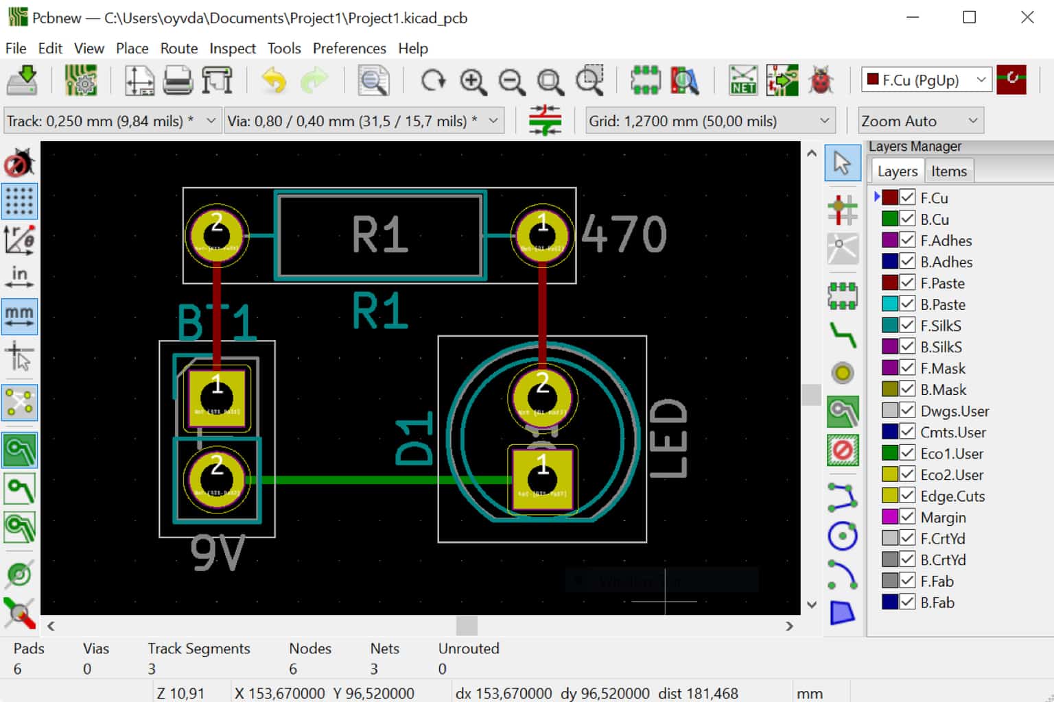
- Draw all the tracks so that you have no more air-wires left
13. Drawing Your Board Outline
Next, draw the outline of your board. To do this, you need to add a polygon on the Edge.Cuts layer.
Click on the Add graphic polygon button on the toolbar, as shown in Image 13.1.

The button for adding a polygon
Select the Edge.Cuts layer.
Click to start drawing the polygon. Click again for each corner. To complete the polygon, click at the point where you started.
- Add a polygon in the Edge.Cuts layer that encloses all your components and tracks
14. Running the Design Rules Check
To check if you’ve made any errors, you need to run the Design Rules Checker – also called the DRC. Typical errors are placing two components too close to each other, or forgetting to draw a track.
The button for running the Design Rules Checker (DRC)
Select the Edge.Cuts layer.
Click on the Design Rules Checker button, shown in Image 14.1, or find it under the Inspect menu. Leave the default options and click on Run DRC button.
Check both the Problems tab and the Unconnected Items tab. The Problems tab will list any design issues, such as a track being too close to another track. The Unconnected Items tab will list any air-wires that you have not yet connected by drawing a track.
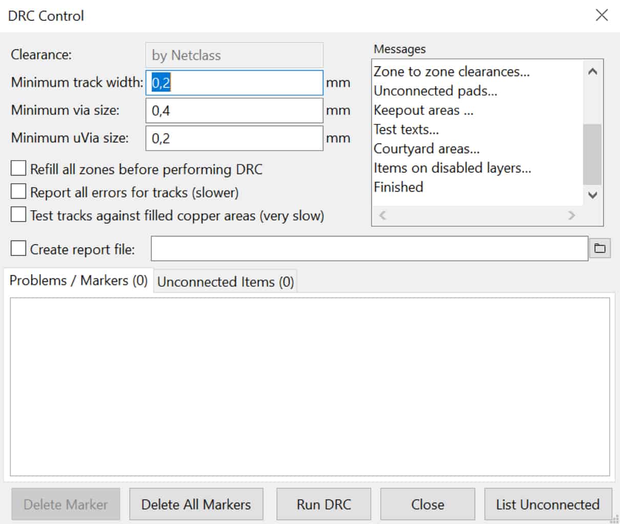
If you see any items on any of these tabs, make sure you fix them before moving on.
If you have a lot of errors, do not despair. Often one little mistake can result in lots of messages. Just focus on one message and try to figure out what it says. Then fix it and run the DRC again.
When you have zero errors listed here, you are done. Your board is finished!
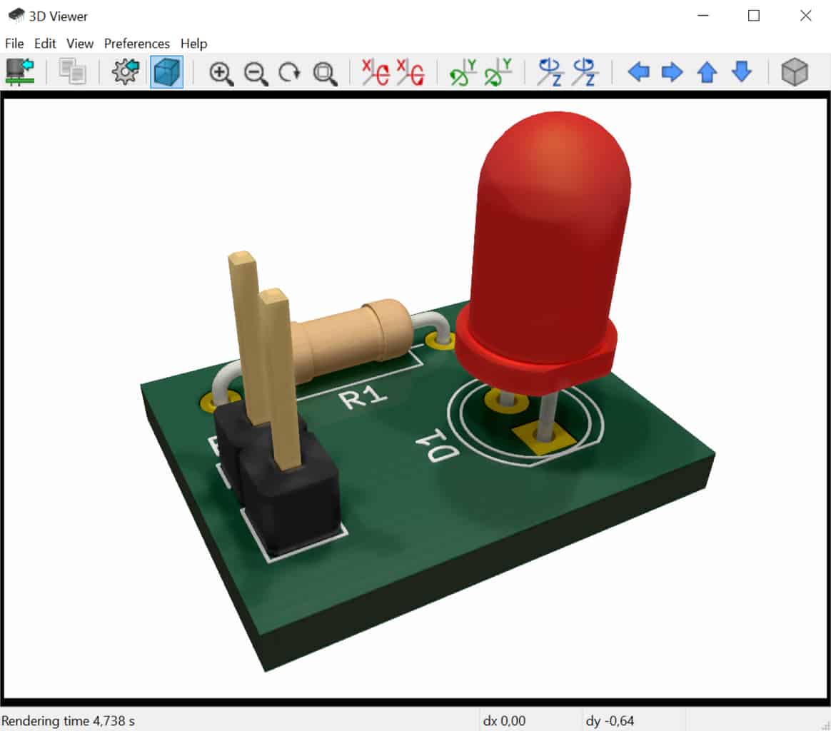
Click on the View menu and select 3D Viewer to see your finished board.
- Run the Design Rules Checker (DRC) and fix any errors that you might have
- Check your design in the 3D Viewer
15. Board Layout Checklist
That’s it for drawing the board layout. To make it easier for your next design, here’s a checklist for all the action points you need to take to complete the board design:
- Open the Board Layout Editor and run Update PCB from schematic
- Place your components in an orderly way
- Draw all the tracks so that you have no more air-wires left
- Create your board edges by adding a polygon in the Edge. Cuts layer that encloses all your components and tracks
- Run the Design Rules Checker (DRC) and fix any errors that you might have
- Check your design in the 3D Viewer
16. How to Get Your Board Made?
You’re now ready to get your board made. This is something that many think is hard and expensive. But that couldn’t be farther from the truth!
These days, PCB manufacturing is available at low cost to anyone who wants to get their circuit boards made. You can find companies that will make a few copies of your boards for only $5-10 (USD).
And it’s become so easy to order that even the most computer-challenged among us can do it.
The Easiest Way
The US manufacturer OSH Park allows you to drag and drop your KiCad PCB file onto their website. That’s it! They process the file in real-time and show you the details of your board so that you can double-check for errors.
Check the file, make the payment, then all you need to do is to sit back and let them make the board for you. The whole process takes less than 5 minutes.
I think we’ll see more manufacturers offering this in the future.
The Traditional Way
The traditional way of submitting your PCB design to a manufacturer is via Gerber and Drill files.
This is a format that all the usable software alternatives for designing PCBs can output, and that all PCB manufacturers can read.
Create Gerber Files in KiCad
From the PCB Editor in KiCad you can create Gerber files by going to the File menu and selecting Plot…
A window will appear.
Click on the Plot button to create the Gerber files.
To create Drill files, click on Generate Drill Files… to open the Drill File dialog. Then click the button Generate Drill File.
There are a lot of options when generating these files. Often the PCB manufacturer you want to use will have instructions on what options to choose.
For more complete instructions, check out How to Create Gerber Files in KiCad.
List of PCB Manufacturers
Here’s a list of a few places you can get your board made:
OSH Park (US)
https://oshpark.com/
Eurocircuits (EU)
https://www.eurocircuits.com/
Seeed Studio Fusion Service (China)
https://www.seeedstudio.com/fusion_pcb.html
PCBWay (China)
https://www.pcbway.com/
jlcpcb.com (China)
https://jlcpcb.com/
allpcb.com (China)
https://www.allpcb.com/
There are many more. Just search for PCB Prototypes or similar on google.
Do You Have Any Questions?
Congratulations, you’ve made it to the end! I really hope this has been helpful. If you have any questions, doubts or feedback, please let me know in the comment section below.
PS! KiCad is constantly being improved upon. Screenshots, library names, or other things from this KiCad tutorial might change over time. If you see something that is no longer as explained in this tutorial, please let me know!
Learn More
A 5-Minute Quickstart Guide to KiCad
How To Edit Symbol in KiCad
How to Create Gerber Files in KiCad
Kicad vs Eagle
Share this tutorial
Hi, I’m Oyvind!
Hey, I’m Oyvind Dahl and I run an electronics membership site for people like you to get really good at building electronics projects. Everything is explained in simple ways and my students learn by doing – not by being swamped with complicated jargon and maths.
Take a look at the course description here https://ohmify.com/
Keep On Soldering!