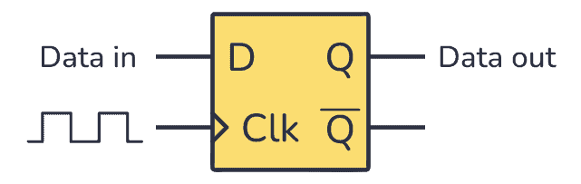
The CD4013 contains two D flip-flops. A D flip-flop stores a 1-bit value and only changes when it receives a clock signal. Specifically, its output pin (Q) changes to whatever is on the input pin D (data) when the clock (CLK) pin goes from LOW to HIGH.
Pin Overview

| Pin Name | Pin # | Type | Description |
|---|---|---|---|
| VDD | 14 | Power | Supply Voltage (+3 to +15V) |
| GND | 7 | Power | Ground (0V) |
| Q1, Q2 | 1, 13 | Output | Outputs from the two D Flip-Flops |
| Q1, Q2 | 2, 12 | Output | Inverted outputs from the two D Flip-Flops |
| CLK1, CLK2 | 3, 11 | Input | Clock input for the two D Flip-Flops (Rising Edge) |
| D1, D2 | 5, 9 | Input | D (data) input for the two D Flip-Flops |
| S1, S2 | 6, 8 | Input | Preset the Flip-Flop output to 1 |
| C1, C2 | 4, 10 | Input | Reset the Flip-Flop output to 0 |
What is a D Flip-Flop?
A D flip-flop is a circuit that can store one bit of data. Its output can either be HIGH or LOW. The output changes to whatever is on the data (D) input when the clock goes from LOW to HIGH. Also called on the rising edge of the clock. (Some D flip-flops change on the falling edge instead.)
This means that the D flip-flop only cares about what is on the data (D) input at the moment this transition happens.
Some D flip-flops have an inverted clock input, which means the output only changes when the clock goes from HIGH to LOW. This is called on the falling edge.
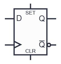
The D flip-flops in the CD4013 also have Set (S) and Clear (C) pins. These can be used to either set the output to HIGH or reset it to LOW, independently of the clock.
A D flip-flop is often used to create shift registers and binary counters, frequency dividers, simple toggling circuits, and much more. See the circuit example further down for a specific use case.
How To Use The CD4013
To be able to use any of the D flip-flops in the chip, you need to first connect the VDD pin to the positive supply terminal and the GND pin to the negative supply terminal.
You can use a power supply voltage between 3V and 15V. Some versions of the 4013 chip support up to 20V. Check the datasheet of your version of the chip for exact values.
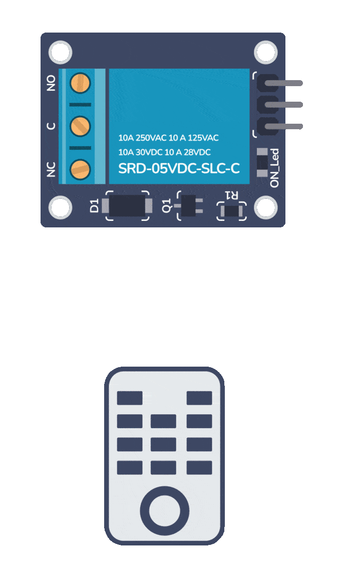
Build Something Useful This Evening
This gadget lets you use any IR remote-control to control your lamp, garden lights, heater oven, garage door, or anything else.
The D (data) pin is where you input the data you want to store in the flip-flop.
Provide a rising edge signal (a signal going from LOW to HIGH) on the CLK pin to store the data from the D pin to the output pin Q.
The output pin Q is always the opposite of pin Q.
Use the S (set) pin to force the output pin HIGH.
Use the R (reset) pin to force the output pin LOW.
CD4013 Example Circuit: Coin Tosser
Here’s an example circuit that you can build with the 4013 Dual D Flip-flop IC – a coin tosser.
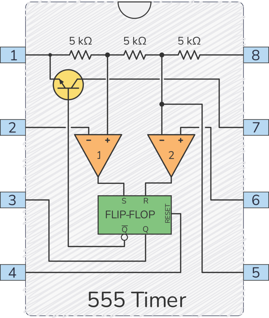
The following circuit uses a 555 timer to create a fast-switching clock signal to the flip-flop when you push the button S1.
The inverted output from the flip-flop is connected back to the D input. This means that for each clock pulse, the flip-flop output will be the opposite of what it was. So it will toggle between HIGH and LOW as long as it receives a continuous clock signal.
The LEDs L1 and L2 symbolize the Heads and Tails of a coin. Since one is connected to the normal output and the other to the inverted output, only one of them will be lit at a time.
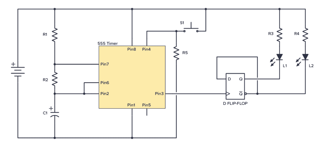
To build this circuit you’ll need:
- A 555 Timer
- A chip with D flip-flops, such as the CD4013BE
- A red and green LED (L1, L2)
- Two 10 kΩ resistors (R3, R4) for the LEDs. (These resistor values depend on your supply voltage)
- A pushbutton (S1)
- A capacitor (C1) – any value from 1 nF to 10 µF should work fine
- Two 1 kΩ resistors (R1, R2)
- One 10k resistor (R5)
- Note: Some versions of the 555 Timer require a 0.01µF capacitor from pin 5 down to ground/minus
- Note: The Set and Clr pins of the D flip flop should be connected to ground to avoid weird behavior from noise
C1, R1, and R2 set the clock frequency from the 555 Timer. Use the following values to create about 48 clock pulses per second (values from our 555 timer calculator):
C1: 10 µF
R1: 1000 Ω
R2: 1000 Ω
R5 is just a pull-down resistor (works similar to a pull-up resistor) to keep pin 4 of the 555 Timer LOW when the button is not pushed. This keeps the 555 Timer in a reset state so that it does not send out any clock pulses.
R5: Can be any value from 10k to 100k Ω
Alternatives and Equivalents for CD4013
You likely find the 4013 IC marked as CD4013, NTE4013, MC14013, HCF4013, TC4013, or HEF4013. Usually with a few extra characters at the end (Ex: CD4013BE).
This has to do with the manufacturer of the chip and the technology used. But the functionality and the pins are the same.
Can’t find any of these chips in your local electronics store? Check out my list of online stores where you can find components and tools for all your electronics projects.
Or try one of the following IC alternatives with D flip-flops:
- 4174: Hex D-type Flip-Flop
- 4175: Quad D-type Flip-Flop
- 40174: Hex D-type Flip-Flop
- 40175: Quad D-type Flip-Flop
- 74HC74: Dual D-type Flip-Flop
- 74HC79: Dual D-type Flip-Flop
4013 Datasheet
Download the PDF datasheet for the IC 4013 here:
CD4013B (Texas Instruments)
HEF4013B (Nexperia)
Go back to the full overview of the 4000-series integrated circuits
10 Simple Steps to Learn Electronics
Electronics is easy when you know what to focus on and what to ignore. Learn what "the basics" really is and how to learn it fast.