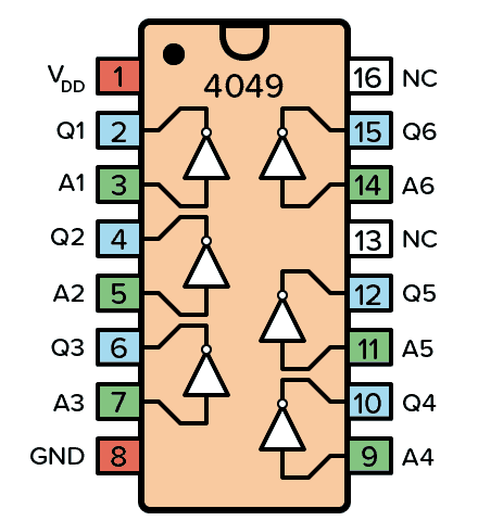
The CD4049 is a hex inverting buffer/converter which basically means that it has 6 NOT gates (inverters) and that it can provide a higher sink current than most logic gates. It has 16 pins, two of which are not in use. This chip is often used for level shifting as it can accept a higher input voltage than its supplied VDD voltage.
Pin Overview
| Pin Name | Pin # | Type | Description |
|---|---|---|---|
| VDD | 1 | Power | Supply Voltage (+3 to +15V) |
| GND | 8 | Power | Ground (0V) |
| Q1-Q6 | 2, 4, 6, 10, 12, 15 | Input | Inputs to the inverters |
| A1-A6 | 3, 5, 7, 9, 11, 14 | Output | Outputs from the inverters |
| NC | 13, 16 | – | Not Connected |
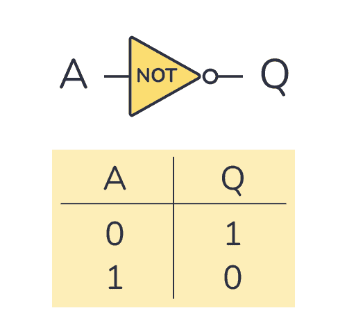
What is a NOT gate/Inverter?
A NOT gate (or inverter) is a logic gate that outputs the opposite of what it gets in. So a 1 (HIGH) on the input will result in a 0 (LOW) on the output.
Click here to learn more about the NOT gate.
What’s special about this chip (compared to other NOT gate chips such as the CD40106 or CD4069) is that it can sink much more current. For example, the CD4049UB from Texas Instruments can sink as much as 48 mA of current.
How to Use the CD4049 in a Circuit?
To use the CD4049 in a circuit, you need a power supply voltage of 3 to 20V (some versions only support up to 15V, so check your datasheet). Connect the power supply to the VDD and GND pins of the chip.
Now you can use any of the six inverters by connecting something to the input and output pins.
That’s it!
Keep in mind that it’s a good practice to connect any unused input pins to either VDD or GND. Leaving them floating can make the gate switch back and forth from noise and thereby use current.
Get the 555 Timer Cheatsheet
A super helpful reference that makes it easy to design circuits, so that you can build oscillators, timer circuits, and more in no time.
CD4049 Example Circuit – High-to-Low Level Shifter
One of the most common application examples for the CD4049 is a level shifter. Let’s say you have a signal with a HIGH level of 10V that you want to connect to an Arduino or other microcontroller that only supports 5V.
To build this circuit, all you need is a 4049 IC:

Since the 4049 contains inverting buffers, you’ll end up with an inverter version of your input. If that’s a problem, simply connect the output to the input of another inverting buffer. The output of the second buffer will be the same as the original but shifted down to 5V logic.
Alternatives and Equivalents for CD4049
The 4049 IC often has a prefix and a suffix, such as CD4049BE, NTE4049, HEF4049, TC4049BP, MC14049, or HCF4049. This is due to the chip manufacturer and the technology used. But the functionality and the pins remain the same.
If you can’t find any of these chips in your local electronics store, check out my list of online stores where you can find components and tools for all your electronics projects.
Can’t find the 4049 anywhere? Then try one of the following IC alternatives:
4049 Datasheet
Download the PDF datasheet for the IC 4049 here:
- CD4049CB (Texas Instruments)
- CD4049UBC (Fairchild Semiconductor)
- HCF4049UB (ST Microelectronics)
- HEF4049B (Nexperia)
Go back to the full overview of the 4000-series integrated circuits
Get the 555 Timer Cheatsheet
A super helpful reference that makes it easy to design circuits, so that you can build oscillators, timer circuits, and more in no time.