A Full Adder is a digital circuit that performs the addition of three binary inputs. In this tutorial, you will learn how this circuit works, its truth table, and how to implement one using logic gates.
What is a Full Adder?
Adders can either be Half Adders or Full Adders. The difference is that the Half Adder is used to add only two 1-bit binary numbers, therefore its sum can only range from 0 to 2. To improve this performance, the Full Adder was developed. It is able to add three 1-bit binary numbers, achieving a sum range from 0 to 3, which can be expressed with two output bits (“11”).
| A | B | Cin | S | Cout |
|---|---|---|---|---|
| 0 | 0 | 0 | 0 | 0 |
| 0 | 0 | 1 | 1 | 0 |
| 0 | 1 | 0 | 1 | 0 |
| 0 | 1 | 1 | 0 | 1 |
| 1 | 0 | 0 | 1 | 0 |
| 1 | 0 | 1 | 0 | 1 |
| 1 | 1 | 0 | 0 | 1 |
| 1 | 1 | 1 | 1 | 1 |
If you follow the above truth table, A and B represent the input variables you want to add, while Cin is a carry input. S is the sum output and Cout is an output to indicate if a carry has occurred. But in binary logic, what does a Carry mean? Well let’s see the next example:
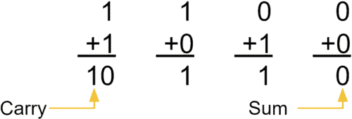
Observe that when you add “0” and “0” or “1” and “0” the result can be expressed with just one bit, but when you add “1” and “1” you need two bits, and one of them is the carry.
But why do you need a carry input in full adders? Well, when you want to sum inputs with more than 1-bit numbers, for example adding two 4-bit binary numbers, you will need to combine several adders and provide a carry input between them to express that the previous less significant operation produced a carry.
The Full Adder Circuit
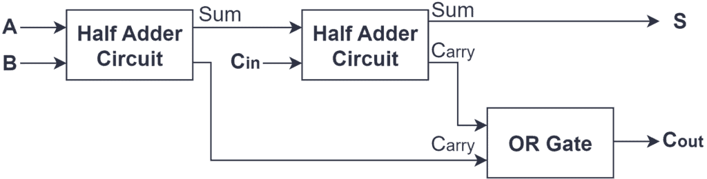
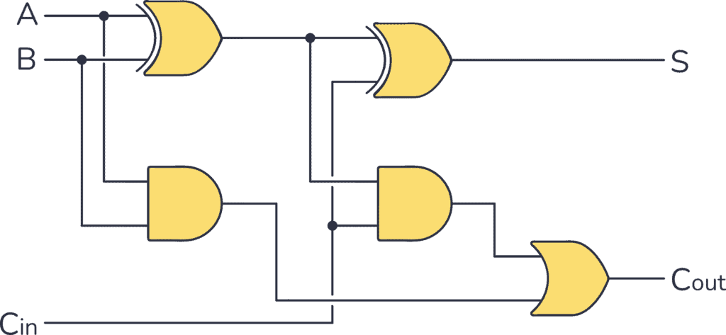
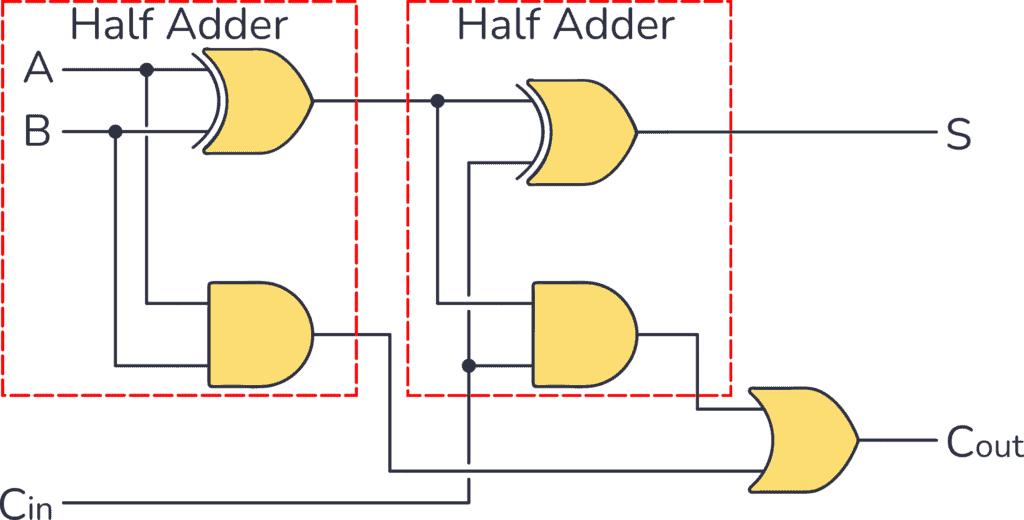
A Full Adder can be built using two Half Adders circuits and an OR gate. The first Half Adder has two 1-bit binary inputs, which are A and B. It produces two outputs; Sum and Carry.
The Sum output of the first Half Adder will be the first input of the second Half Adder. And the Carry output of the first Half Adder will be the second input to the additional OR gate.
The second input of the second Half Adder becomes the Carry input (Cin) of the Full Adder.

10 Simple Steps to Learn Electronics
Electronics is easy when you know what to focus on and what to ignore. Learn what "the basics" really is and how to learn it fast.
The second Half Adder will also provide Sum and Carry outputs. Its Sum output represents the Sum output (S) of the Full Adder, and its Carry output is the first input of the additional OR gate. Finally, the OR gate will generate the Carry output (Cout) of the Full Adder.
Let’s replace the blocks with the actual circuits:
Applications of the Full Adder: 4-bit Binary Adder
Let’s suppose you want to add the following two 4-bit binary numbers A and B:
A = 1111 B = 1111
The result will be a 5-bit number:
11110
Where the most significant bit indicates a carry.
So in order to add two 4-bit binary numbers as above, you will need to combine four Full Adders as follows:
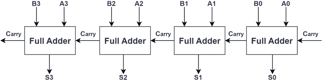
As you can see, the inputs A and B of each adder contain the elements of the two 4-bit binary numbers, distributed from their less significant bits from right to left. Also, observe how the carry output of one Full Adder is the carry input of the next one. Just remember this is to take into account if the previous less significant operation produced a carry.
Check out the CMOS CD4008 chip that can add two 4-bit binary numbers.
Questions?
Do you have any questions about the Full Adder? Let me know in the comments below.
More Digital Electronics Tutorials

Oyvind's Circuit Tips
Get my tips for learning electronics, curious circuits, useful tutorials, hints for choosing components and much more via email.
